www.igglybob.com
r.e.t.a.r.d.
The Core

the main

 - main page
 - about me
 - l.o.u.n.g.e.
 - r.e.t.a.r.d.
 - s.o.l. meter
 - s.c.r.e.a.m.
 - videos

the l.o.u.n.g.e.

 - overview
 - 2006 edition
 - 2007 edition
 - 2008 edition
 - control

the s.c.r.e.a.m.

 - main page
 - tech review
 - proposal
 - draft summary

the r.e.t.a.r.d.

 - overview
 - assignment
 - proposal
 - requirements
 - timeline
 - the core

the s.o.l. meter

 - overview
 - car modification
 - meter design
 - meter input

I. Introduction

    The R.E.T.A.R.D. is composed of both input/output regions and an internal processor (which will be referred to herein as 'the core' or 'the R.E.T.A.R.D. core'). The functionality of the input/output, as seen by the user, was described in the proposal. However, the functionality and architecture of the internal processor itself was not defined in the proposal; this document aims to clarify the internal processor's structure and abilities.

II. Basic Architecture and Flow

    The R.E.T.A.R.D. core is made up of the same elements as most CPUs; however, it is certainly not the same. The most notable feature of the R.E.T.A.R.D. core is that it is capable of loading a register from RAM and executing an operation on two registers concurrently. To allow this, the RAM was not connected to the output of the register file (which is what is done in a simple single cycle datapath). Instead, it has a separate channel of communication with the register file and the instruction decoder. This also eliminates the need for an immediate register. The equivalent method of an immediate add would then be to load a value into a register before an add instruction. The loading would be done concurrently with the previous instruction, so the R.E.T.A.R.D. core's implementation of an immediate add is not slower than a CPU with an immediate register.

    A register transfer level schematic of the R.E.T.A.R.D. core can be seen in Figure 1, and it can be compared with an equivalent schematic of a simple single cycle datapath in Figure 2.


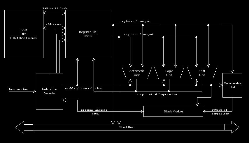
Figure 1. RTL schematic of the R.E.T.A.R.D. core.


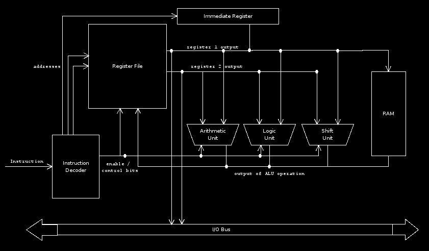
Figure 2. RTL schematic of a simple single cycle datapath.

III. ISA (Instruction Set Architecture) and Assembly Specification

    The instructions accepted by the R.E.T.A.R.D. core are similar to those accepted by most instruction sets, though it has less instructions than most. The number of instructions are few to keep the complexity of the core low, which also serves to keep the cost of the FPGA the R.E.T.A.R.D. core will be implemented on down. As discussed earlier, the R.E.T.A.R.D. core has no immediate register; therefore, instructions involving immediate registers are not required and do not exist in the ISA. However, instructions do exist to load values directly into RAM or a register. Table 1 details all the instructions accepted by the R.E.T.A.R.D. core, their syntax, and a description of what they do. Due to the large amount of addressing space it takes to concurrently load a memory value and perform an operation, most operations store their output in one of the registers passed as input. Any programmer with basic thinking skills should be able to use this, and clever programmers should be able to use it to their advantage.

Opcode Instruction Syntax Description
00000 no-op nop No operation: do nothing.
00001 add add $1 $2 Add the contents of registers $1 and $2, storing the result in register $1.
00010 subtract sub $1 $2 Subtract register $2 from register $1 ($1 - $2 = result), storing the result in register $1.
00011 logical and and $1 $2 Logically and registers $1 and $2, storing the result in register $1.
00100 logical nand nand $1 $2 Logically nand registers $1 and $2, storing the result in register $1.
00101 logical or or $1 $2 Logically or registers $1 and $2, storing the result in register $1.
00110 logical nor nor $1 $2 Logically nor registers $1 and $2, storing the result in register $1.
00111 logical xor xor $1 $2 Logically xor registers $1 and $2, storing the result in register $1.
01000 logical not not $1 $2 Take the logical inverse of register $1, storing the result in register $2.
01001 shift left logical sll $1 $2 Shift register $1 left logically by the amount of bits specified in register $2. The output is stored in register $1.
01010 shift right logical srl $1 $2 Shift register $1 right logically by the amount of bits specified in register $2. The output is stored in register $1.
01011 shift left arithmetic sla $1 $2 Shift register $1 left arithmetically by the amount of bits specified in register $2. The output is stored in register $1.
01100 shift right arithmetic sra $1 $2 Shift register $1 right arithmetically by the amount of bits specified in register $2. The output is stored in register $1.
01101 rotate left rol $1 $2 Rotate register $1 left by the amount specified in register $2. The output is stored in register $1.
01110 rotate right ror $1 $2 Rotate register $1 right by the amount specified in register $2. The output is stored in register $1.
01111 copy register copy $1 $2 Copy the contents of register $1 into register $2.
10000 jump jump $(val) Jump to the program memory address $(val), where $(val) is a 22-bit address. This instruction cannot be streamlined with a RAM load/write operation.
10001 jump on zero jzero $1 $(val) If the contents of register $1 are zero, jump to the program memory address $(val), where $(val) is a 22-bit address. This instruction cannot be streamlined with a RAM load/write operation.
10010 jump on positive jpos $1 $(val) If the contents of register $1 are positive, jump to the program memory address $(val), where $(val) is a 22-bit address. This instruction cannot be streamlined with a RAM load/write operation.
10011 jump on negative jneg $1 $(val) If the contents of register $1 are negative, jump to the program memory address $(val), where $(val) is a 22-bit address. This instruction cannot be streamlined with a RAM load/write operation.
10100 call call $(val) Jump to the program memory location at $(val), pushing the current program memory location onto the stack. $(val) is a 22-bit address. This instruction cannot be streamlined with a RAM load/write operation.
10101 return return Return to whatever program memory location is on top of the stack. This operation can be streamlined with a RAM load/write operation.
10110 increment inc $1 $2 Increment register $1 by 1, storing the output in register $2.
10111 decrement dec $1 $2 Decrement register $1 by 1, storing the output in register $2.
11000 load immediate value lim $1 [value] Load [value] into register $1, where [value] is a 22-bit two's complement integer. RAM load/write operations cannot be streamlined with this operation.
11001 get input in $ioaddr $flags $1 Get input from the device at $ioaddr (3 bit code) on the Short Bus and store it in register $1. The variable $flags is a 2-bit variable that is sent to the I/O device.
11010 send output out $ioaddr $flags $1 Send the contents of register $1 to the device at $ioaddr (3 bit code) on the Short Bus, also sending $flags (2 bits) to the device on the Short Bus.
load from RAM load $1 $ramaddr Load the value stored in RAM at $ramaddr (10 bits) into register $1. This operation has no opcode because it is performed concurrently with other operations. However, it cannot be performed concurrently with a write operation.
write to RAM write $1 $ramaddr Write the value stored in register $1 to $ramaddr (10 bits). This operation has no opcode because it is performed concurrently with other operations. However, it cannot be performed concurrently with a load operation.

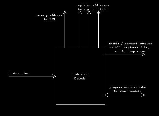
IV. Input/Output of the R.E.T.A.R.D. Core (the Short Bus)

    As discussed in the original proposal, the R.E.T.A.R.D. will communicate with other devices solely over the Short Bus. The Short Bus is a 37-bit bus through which all the devices contained in the R.E.T.A.R.D. are connected. It is a master-slave bus, where the R.E.T.A.R.D. core is the master and is the only device allowed to control the first 5 bits, which are the control bits. All other devices can only respond to control requests and put data on the other 32 bits of the bus. The first 3 bits are used for addressing specific devices; this allows for up to 7 devices (not including the R.E.T.A.R.D. core itself), which is sufficient for the project. The next 2 bits specify flags that are being passed to the device. Each device accepts different flags for different functions, and will respond differently. Specific information about how each device will respond to flags is not defined in this document. Figure 3 shows how the Short Bus interconnects all the devices to the R.E.T.A.R.D. core.


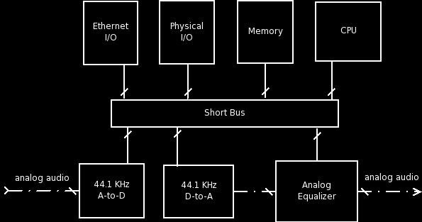
Figure 3. Block diagram of the R.E.T.A.R.D.

V. Clock / Timing Issues

    Due to the architecture of the R.E.T.A.R.D. core, each instruction cannot be performed in one clock cycle. However, each instruction will take the same amount of clock cycles to complete, to simplify timing issues. Also, to simplify timing issues, the instruction decoder will be clocked at a fraction of the frequency of the other components. By doing this, the instruction decoder does not need to store information about what it is waiting on, since it will begin each clock cycle by fetching the next instruction. Therefore, the R.E.T.A.R.D. core is not a state machine, making it different from many other processors.

VI. Detailed Description of Core Components

  a. Instruction Decoder
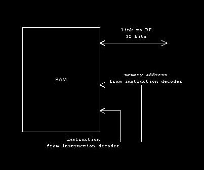
    This component is the main controller of the R.E.T.A.R.D. core. At the beginning of each clock cycle, it reads the next instruction. It decodes it, and will set outputs to the register file, RAM, ALU, and stack accordingly. It should be noted that this controller will be clocked at a lower speed than the other components (see section IV).

Figure 4. I/O diagram of the instruction decoder.


  b. RAM

    The RAM stores runtime program memory. It does not store the program instructions themselves, though. It is accessed by the instruction decoder and register file, and is capable of writing a memory value to a register or reading a register value and writing that value to a memory location. Because the formatting of the R.E.T.A.R.D. core's instructions, there are only 1024 addressable 32-bit words. This gives a total of 4096 bytes of RAM, which is a small amount but should be sufficient.

Figure 5. I/O diagram of the RAM module.


  c. Register File

    The register file of the R.E.T.A.R.D. core is different than most register files. It accepts addresses for three registers, outputs three registers, and is capable of writing two registers at once. If the same address is given for both write registers, the logical or of both write registers will be written to the specified address. This behavior results from an attempt to keep the register file's implementation as simple as possible.

Figure 6. I/O diagram of register file.

  d. ALU

    The ALU is actually three smaller components: an arithmetic unit, a logic unit, and a shift unit. Each of these components is capable of what its name might imply; the arithmetic unit adds, subtracts, increments, or decrements input; the logic unit performs logical operations on two input registers; the shift unit performs shifting and rotating operations. This is functionally equivalent to the ALU in the simple single cycle datapath.


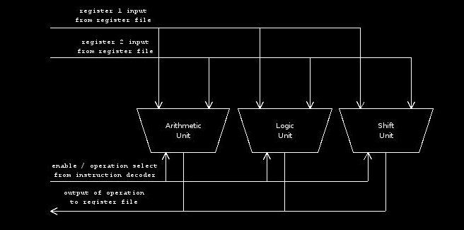
Figure 7. I/O diagram of ALU.

  e. Comparator

    The comparator is a rather simple component. Its purpose is to make comparisons for commands like 'jpos', 'jzero', and 'jneg'. It accepts one register as input, and depending on the control input given by the instruction decoder, it will output whether or not the number is equal to zero, greater than zero, or less than zero. This output will be acted upon by the stack module.

Figure 8. I/O diagram of comparator module.

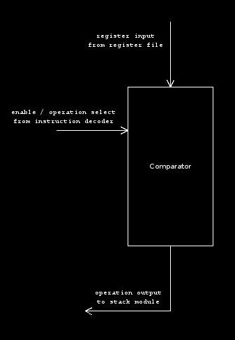
  f. Stack Module

    The stack module holds information about the memory addresses currently on the stack. It receives input from the instruction decoder and the comparator. It is capable of adding registers to the stack and removing them from the stack. The stack length is up to 8 levels long; recursion will not be necessary.


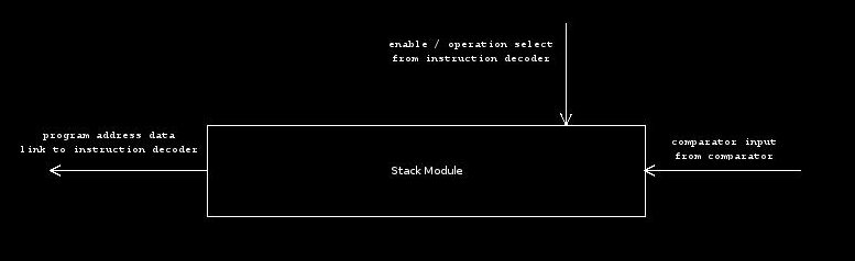
Figure 9. I/O diagram of stack module.

VII. References and Useful links

[1]. R.E.T.A.R.D. Project Proposal - http://www.igglybob.com/projects/retard/proposal.php
[2]. Project Timeline - http://www.igglybob.com/projects/retard/project_timeline.php
[3]. Requirements and Test Document - http://www.igglybob.com/projects/retard/requirements.php